
| 高周波挿入損失、RLGC、Sパラメータを抽出するSi9000e PCBフィールドソルバー 英文カタログ | |
| ビデオ解説(英語)Click here | |
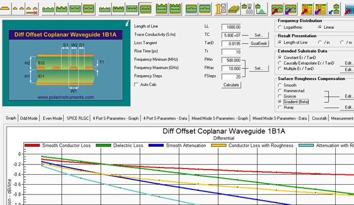
| Si9000e は、スピーディに高精度なPCB 伝送線路シミュレーションモデリングを可能にします。 伝送線路損失、周波数ドメインでの特性インピーダンスシミュレーション結果をモデル化し、200近くの伝送線路モデル構造をシミュレーション可能で広範囲にわたって伝送線路パラメータ全体を抽出できるように設計されています。境界要素法(BEM)フィールドソルビングを採用した Si9000e は、RLGC マトリックスを抽出し、伝送線路構造内の情報をスピーディーにプロットします。挿入損失は、誘電損失、導体損失、表面粗化損失、全損失が一目でわかる3通りの方法でグラフ化され、Huray / Canonball /Gradient法 に加えて、表面粗化処理モデリング用の従来の Hammerstad法 および Groisse法も追加されました。 Polar層構成シミュレーションSpeedstackにリンクさせ Speedstack Si としても使用可能です。 | |
| Speedstack SiとしてSpeedstackとリンク可能 Si クロストーク オプション – 複数のライン、差動ペア(挿入損失を考慮しない)クロストーク – トレース間のカップリングをモデル化 Si プロジェクト オプション Speedstackで伝送線路構造をグループ化して保存(同じ基板上で挿入損失値を比較など可能) 表面粗化モデリング – Cannonball-Huray / Gradient / Hammerstad / Groisse 法 表面粗化パラメータデータ Rz (Canonball-Huray) / RMS (Rq) 水平面に対する傾きの度合い ビルトインインピーダンスグラフ 導体損失・誘電体損失の挿入損失値を個別にグラフ化できます 一目でわかる Sパラメータチャート – 振幅、位相、スミスチャート シングルエンドとミックスモードの Sパラメータのグラフチャートとデータ表 ユーザー定義のSパラメータ形式と終端インピーダンス 1KHz以上からの周波数依存性モデリング 差動ビアの計算機能 カラー表示によるビアスタブチェック機能 | |
| Si9000eは、全損失、導体損失、誘電体損失の挿入損失をグラフ化できます。Si9000eは、複数の誘電体材料の組み合わせた複合材料に対応し、ソルダレジストの影響も考慮して計算する機能も持ちます。ソルダレジスト厚の設定は、トレースの横、トレース間、トレースの上それぞれを個別に設定できます。多くの Polarユーザー客が、特に伝送ライン挿入損失に関する周波数依存インピーダンス値モデリングを要望しており、その結果が Si9000eが開発されました。 Si9000eは、Si8000mと同様にPCB製造業界標準の、境界要素法(BEM)プラットフォーム上に構築されています。多くのエンジニアが、伝送線路インピーダンスの設計ツールとしてSi8000m を使用していますが、Si9000eは、Si8000mをベースに機能を拡張して強化された伝送ラインパラメータを出力します。 | |
| 差動ビア計算機能 / ビアスタブチェック機能 Si9000eの機能: 差動ビアのインピーダンス計算は、差動のPTH(めっきスルーホールビア)をモデル化して正確に回路モデルを計算できます。 ビアスタブチェックは、ビアスタブの信号歪み効果を考慮したシグナルインテグリティの状態を色で示します。スタブ長と Er値が増加して、信号の立ち上がり速度が速くなると、スタブによるシグナルインテグリティへの悪影響が大きくなります。Si9000e ビアスタブチェックは、3通りの方式をサポートしています: 1.スタブ長、実行誘電率、ビットレート周波数による計算 2.スタブ長、実行誘電率、周波数帯域による計算 3.スタブ長、実行誘電率、立ち上がり速度による計算 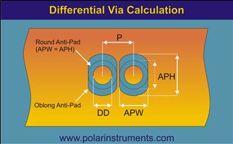  差動ビア計算 ビアスタブチェック 差動ビア計算 Polarアプリケーションノート AP8204.pdf (Bert Simonovich によるデザインノート) 差動スルーホールビアのスピーディで高精度な回路モデリングを実現するシンプルで実用的な方法論。 Dielectric Anisotropy(誘電異方性)について ビアスタブチェック Polarアプリケーションノート AP8166 (ビア、スタブの高速信号に対する悪影響の最小化) では、要求されるビットレート・周波数で、ビア・スタブの影響を軽減または除去するための手順が必要かどうかを確認する方法について説明しています。 実用的な S-パラメータ グラフ作成 Si9000e PCB 挿入損失フィールド ソルバーは、2 ポート・ 4 ポートの フルレンジ S パラメータを 1 つのチャート ウィンドウ上で表示します。 Click on the links below to display the full range of 4-port S-parameters data series, S11 – S44. Magnitude Smith chart Mixed mode The Si9000e provides a comprehensive range of data presentation in both tabular and chart form with the option of single-ended and mixed-mode S-parameters. 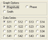 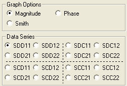 The differential S-parameters, SDD11, for an edge-coupled surface microstrip are shown below. 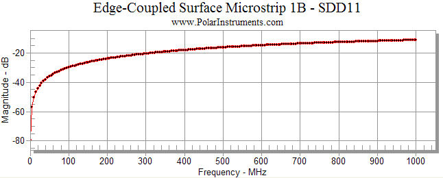 Frequency-dependent calculations Employing its Boundary Element Method field solving, the Si9000e extracts RLGC matrices and 2-Port (single-ended) or 4-Port (differential) S-Parameters and rapidly plots transmission line information for the structure under design. Graphing against frequency is provided for impedance magnitude, loss (conductor loss, dielectric loss and insertion loss), inductance, capacitance, resistance, conductance and skin depth. The Polar Si9000e runs within the Microsoft Windows environment and provides for simple transfer of table data to external programs such as spreadsheets or databases for subsequent analysis. Si9000e graphs Impedance v Frequency 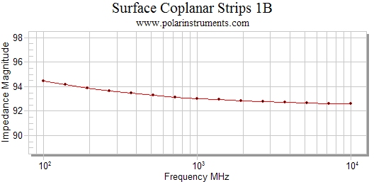 Impedance magnitude with frequency Conductance v Frequency 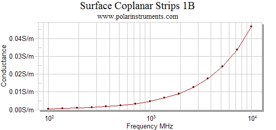 Conductance v frequency Skin depth v Frequency 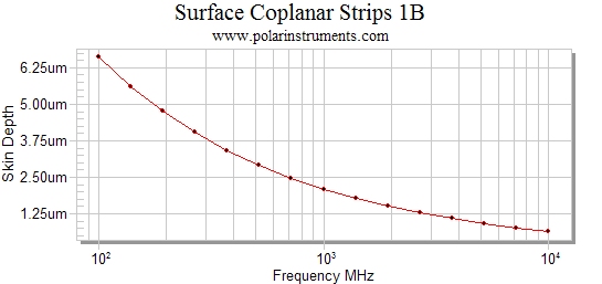 Skin depth v frequency Extended substrate tables The Si9000e frequency-dependent calculations can be refined using extended substrate data. Assign substrate values by frequency band to accommodate material from manufacturers who specify parameters that vary by frequency. Manufacturers may specify, for example, differing values of Er and loss tangent across a range of frequencies. 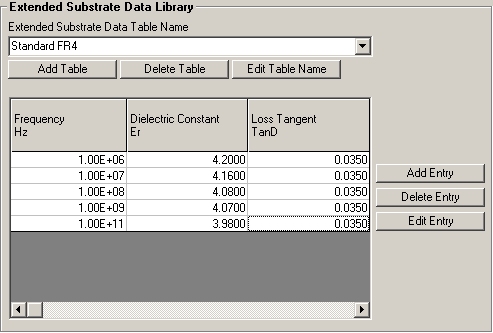 Extended substrate data tables Frequency dependent calculation range For frequency dependent calculations the Si9000e calculation engine supports lower frequencies down to 1KHz. 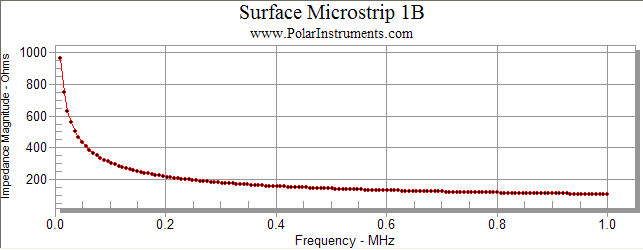 High layer-count builds For those working with complex high layer-count builds the Si9000e also links to the Polar Speedstack PCB Stackup Design System and is available in the Speedstack Si package. Using the Speedstack Si allows you to keep all your stack design data in one convenient file – and you can draw library material from your fabricator or from base material suppliers in the Polar Material Partner program. Designed to save you time compared with traditional methods, the Si9000e lets you choose graphically the structure you need to model and enter the geometric and material data and the range of frequencies under analysis. Select the graphs or table you need and the Si9000e solves for the results. Advanced users may also enter available data for Er and TanD versus frequency – the Si9000e will take these into account. シングルエンド構造: 差動構造: Support Please take a look at the Signal Integrity / Loss Application Notes – you will gain maximum benefit from your Si9000e if you read these supporting notes. These brief articles help you translate the precision output of your field solver into practical real world PCBs with good production yields. Ask us about support packages for your Si9000e. System requirements For PC system requirements for Si9000e see AP605 Si Excel pre-prepared Microsoft Excel workbooks option XML Interface Module Si Crosstalk multi line and differential pair (lossless) crosstalk option Speedstack / Field Solver options License options Polarcare brochure | |